


27, Aug 2026
Aime Unveils Bold New Brand Identity as It Enters Its Next Chapter of Growth
AIME has revealed a new brand identity marking a fresh chapter for Asia Pacific’s largest and longest-running business events trade show as it enters its 34th year. Coming off five consecutive years of growth, AIME has built a global profile as the show that international buyers, exhibitors and industry leaders return to year after year.
The rebrand signals the beginning of a new chapter for AIME, reflecting its growth ambitions and reinforcing the event’s position as one of the premier global business events industry gatherings.
The refreshed look is bolder, brighter and more contemporary, built around the tagline “Bring your ambition to Melbourne. Share it with the world.” At its centre is a new symbol formed from directional shapes that subtly spell out AIME.
The AIME brandmark reflects a modern, forward-thinking event and features a vibrant colour palette, refreshed imagery and motion design. The AIME symbol represents the strength of connection inherent to AIME and draws on Melbourne’s floral emblem, the native Paper Daisy. The flower’s resilience aligns with AIME’s purpose: the global industry coming together to create something stronger.
Melbourne Convention Bureau CEO Julia Swanson says the brand evolution reflects AIME’s growing global standing.
“AIME has been the premier platform where international decision-makers connect and build long-term value in Melbourne. As the owners of AIME, MCB is proud to see the event’s identity evolve. The new brand matches the ambition, energy and personality of the show itself, while underscoring AIME’s role in driving real economic and intellectual growth across the globe.”
Talk2 Media & Events was commissioned to manage AIME in 2019, and CEO Matt Pearce says AIME’s evolution and growth over years have shaped the brief for its new brand.
“Every year, more than 5,000 people gather for AIME. They come from around the world to build relationships, trade ideas and forge the connections that drive the multi-billion-dollar global meetings, conventions and exhibitions industry forward. Then they disperse across the world, carrying what they learned at AIME back into their own markets and their own work.”
AIME Marketing Director Monica Kent-Giles says the refresh moves the brand into a bolder, more contemporary space.
“We wanted an identity that feels modern, elevated and distinctly AIME. All the design elements, from the custom typography and colour palette to the versatile new symbol, give us a sophisticated, expressive visual toolkit. The refresh honours AIME’s heritage while delivering a brand identity that aligns with where the show is heading.”
AIME Event Director Silke Calder says the brand refresh aligns with the show expanding to its largest ever footprint as the domestic and international Hosted Buyer program opens.
“At its core, the team set out to create a new identity that is contemporary and confident, a fresh take on what AIME is. AIME has always been about the strength of community and the magic that happens when people come together to collaborate and exchange ideas. This new brand identity comes at the perfect time as we build towards another record-breaking year for buyers and exhibitors.”
Alongside the new brand, applications are now open for the AIME 2027 Hosted Buyer Program, inviting qualified corporate event planners, incentive specialists and Professional Conference Organisers to experience Asia Pacific’s premier business events platform first-hand. The program pairs expert human curation with AI to deliver tailored, pre-scheduled appointments with top-tier global exhibitors.
Approved Hosted Buyers receive a fully supported attendance package: complimentary return flights, accommodation and a custom appointment diary, plus access to the Knowledge Monday program, networking events and the annual Welcome Event.
The new branding produced in partnership with Studio Quarantine will roll out across all event touchpoints, digital platforms and marketing campaigns in the lead-up to AIME 2027, returning to the Melbourne Convention and Exhibition Centre (MCEC) 15-17 February 2027.
- 0
- By Neel Achary

26, Aug 2026
Rackspace Technology Launches Rackspace Cloud, Among the First Fully Managed Multitenant Cloud Platforms Built on VMware Cloud Foundation 9.1
New platform gives enterprises elastic VMware capacity ready for virtual machines, Kubernetes, and production AI workloads, with the governance and control regulated industries require
SAN ANTONIO, TX – Aug 26 – Rackspace Technology® (NASDAQ: RXT), a global enterprise AI infrastructure and solutions provider, announced the launch of Rackspace Cloud, a fully managed, multitenant cloud platform powered by Broadcom’s VMware Cloud Foundation 9.1 (VCF 9.1), initially available in Dallas, followed soon by North Virginia and Chicago areas. Rackspace is among the first providers to bring a fully managed multitenant platform to market on VCF 9.1, and one of a limited set of Broadcom Advantage Partners able to deliver VCF-based managed cloud services. Rackspace Cloud gives enterprises a new way to use modern cloud capabilities, such as Kubernetes and containerized applications, while maintaining the VMware environment and control they require.
The launch arrives as enterprise demand shifts decisively toward governed private infrastructure. Broadcom’s Private Cloud Outlook 2026 research found that 56 percent of organizations are running or planning to run production AI inferencing in a private cloud, while public cloud use for production inference declined 15 percent year over year from 56 percent to 41 percent.
“For years organizations operating private clouds have had to choose between agility or control,” said Bryan Litchford, Head of Product, Engineering, and Data Centers at Rackspace. “Rackspace Cloud removes that tradeoff. The same governed platform that powers an enterprise’s VMware environment today provides the flexibility to support Kubernetes and AI inference workloads as business needs evolve, all while maintaining consistent governance and control. With capacity staged in advance, automated lifecycle management, and enterprise-grade VMware capabilities delivered through a fully managed service, customers scale in hours, not procurement cycles.”
“Rackspace Cloud powered by VMware Cloud Foundation gives customers a managed path to cloud agility, combining Rackspace’s operational expertise with Broadcom’s leading private cloud platform,” said Ricky Cooper, Vice President of Global Cloud Service Providers, OEM and eOEM, Broadcom. “Together, we are helping enterprises scale their modern private clouds cost-effectively, operate securely, and innovate rapidly.”
As enterprises evaluate modernization strategies and seek alternatives to increasingly complex environments, Rackspace Cloud simplifies VMware operations, speeds deployments, and reduces the burden of buying hardware and maintaining data center infrastructure, without requiring customers to manage the underlying systems or buy additional capacity.
Key capabilities include elastic consumption on pre-staged infrastructure, integrated support for virtual machines and Kubernetes workloads on a single platform, and enterprise grade isolation, security, and governance controls. The platform is delivered with transparent lifecycle management, multiple performance tiers, and 24x7x365 managed operations.
Rackspace will showcase Rackspace Cloud at VMware Explore 2026 in Las Vegas, August 31 through September 3, where Rackspace is a Diamond Sponsor exhibiting at Booth #104, and will be presenting in the session, “VCF State of the Union: Optimizing Costs and Closing Security Gaps in the AI Era [CLOB1276LV].”
For more information, visit https://www.rackspace.com/enterprise-ai/partners/vmware.
26, Aug 2026
Artificial Intelligence is Transforming Asset Managers’ Risk Management Models, Clearwater Analytics Research Reveals
BOISE, Idaho, NEW YORK, CHICAGO, LONDON and HONG KONG, Aug 26: Artificial intelligence (AI) is transforming key components of asset managers’ operational processes, and nowhere is that more evident than in their risk management practices, new research from Clearwater Analytics shows. For an industry where speed and precision of risk identification often determines whether exposure is managed or missed, the shift AI is driving matters well beyond efficiency.
Almost all fund managers (95%) surveyed across a broad spectrum of fund managers including insurance asset managers, hedge funds, private markets specialists, and general asset managers, have seen improvements in the level of real-time insights being generated since adopting AI into their risk management systems, while 17% said those changes had been dramatic.
Managers using AI in risk management in this function want to develop a more proactive model, one built to predict and prevent risk in real time. Almost a third (32%) said their process had become much more proactive, while a further 60% said they had seen a slight increase in proactivity. Only 8% had seen no change from using AI.
Predictive analytics is where the shift becomes most concrete. AI offers the ability for managers to develop their risk management systems to deliver greater predictive analytics. Supported by machine-learning models that can analyze vast data sets to identify patterns and predict future trends with greater accuracy than traditional methods, this will be highly beneficial for forecasting risk
Since they began to use AI, the vast majority of fund managers (87%) said their ability to use predictive analytics as part of their risk management had improved, with a fifth (20%) claiming the improvement was dramatic. Some (12%) had seen no change, and only 1% said it had worsened.
The gains extend into reporting as well. In addition to offering better predictions, 88% of managers said the ability to process vast amounts of data had increased the turnaround of regulatory and accounting reports. Almost half (42%) said they had increased the speed of report production by between 10% and 24%, while a further 30% said it had increased between 25% and 49%. Almost a tenth (9%) had seen the speed they could generate reports increase by between 50% and 74%.
Manual reconciliation tells a similar story. More than half of managers (55%) have seen a reduction in the need for manual reconciliations. A fifth (20%) have seen these reduce by up to10%, 19% have seen them reduce between 10% and 24%, and 15% have been rewarded with reductions of between 25% and 49%.
Only 2% of managers said they had not yet used AI within this function. Almost a quarter (24%) said using AI had actually slowed their process down, a reminder that these gains depend on how well the technology is implemented, not simply on whether it’s adopted.
26, Aug 2026
Algorand Foundation Launches AC2: An Open Protocol for Secure, User-Controlled Communication with AI Agents
New open standard puts users in control of AI-driven signing operations, enabling secure agentic commerce without exposing private keys
Dover, Delaware, Aug 26 —Algorand Foundation announced the public launch of AC2 (Agentic Communication and Control Protocol), an open-source, blockchain-agnostic standard for secure peer-to-peer communication between users and AI agents. The specification and reference implementation are available now atgithub.com/algorandfoundation/ac2.
As AI agents increasingly execute payments, sign code, and manage digital operations on behalf of users, existing messaging channels (e.g., email, Telegram, WhatsApp) offer no cryptographic identity verification, no standardized delegation, and no way for users to approve individual actions without handing over their private keys entirely. AC2 closes that gap.
The protocol establishes a direct, end-to-end encrypted WebRTC connection between a user’s wallet or app and an AI agent. When an agent needs to perform a signing operation – a payment, a git commit, an API authorization – it sends a request to the user via AC2. The user reviews and approves through their own wallet interface, and the signature is delegated back to the agent. The private key never leaves the user’s control.
“AC2 is Algorand’s answer to a fundamental question the industry has been sidestepping: how do you give AI agents the authority they need to be useful, without the authority to act against your interests?” said Marc Vanlerberghe, Chief Strategy and Marketing Officer at the Algorand Foundation. “The answer is you don’t hand them the keys, you approve each use of them.”
AC2 supports a broad range of agentic workflows. A coding agent can draft code and ask the developer to approve the final digital signature before it’s published. Similarly, an AI assistant can manage payments by sending the transaction details directly to a users’ digital wallet, where they can easily review and approve them before the payment goes through. A shopping agent can construct an AP2 Intent Mandate, defining what it is authorized to buy and at what price, then submit it to the user for sign-off before acting autonomously. Because AC2 supports extensions, any message type or signing format can be added to the protocol, making it suitable for any domain where agents need scoped, user-approved authority.
AC2 uses DIDComm v2.0 message formats to ensure seamless operability across different systems, passkey-based authentication via Liquid Auth (built on FIDO2/WebAuthn), and supports real-time voice and text streaming as well as signing delegation. It requires no central message relay and no blockchain to operate.
Alongside the specification, the Foundation is releasing an open-source wallet proof-of-concept and an OpenClaw plugin for end-to-end developer testing. The Foundation is actively inviting design partners to review and contribute to the AC2 spec.
-
Specification and code:github.com/algorandfoundation/ac2
-
Website: ac2protocol.org
-
Contact:press@algorand.foundation
26, Aug 2026
AAEON Announces Plans to Incorporate NVIDIA Jetson Orin Nano 2 Module into its Embedded AI System Roadmap
Following the announcement of NVIDIA Jetson Orin Nano 2, AAEON confirmed it will support the adoption of the module through its BOXER-8XXXAI product line.
Taipei, Taiwan – Aug 26: Following the announcement of NVIDIA Jetson Orin Nano 2, industry-leading edge AI platform provider AAEON (Stock Code: 6579) has announced its intention to integrate the energy-efficient, compact module into its Fanless Embedded AI System range.
NVIDIA Jetson Orin Nano 2, which will feature twice the performance of its predecessor and consumes much less power at the same performance, is to be made available in both module and developer kit form during the first half of next year.
In response to the news, AAEON has confirmed that it is one of the ecosystem partners working with NVIDIA to adopt the new addition to the NVIDIA Jetson Orin series modules, noting that a more detailed product roadmap with system-level specifications will be announced closer to the module’s official market release.
Powered by an NVIDIA Ampere architecture GPU with 1,536 CUDA Cores and improved Tensor Cores, NVIDIA Jetson Orin Nano 2 will provide up to 78 TOPS of AI performance. Meanwhile, the module will also include an 8-core Arm Cortex CPU and 8GB of LPDDR5x with higher memory bandwidth.
For AAEON customers seeking robust hardware platforms to build entry-level edge AI solutions across physical AI, one of the key benefits of NVIDIA Jetson Orin Nano 2 will be its optimized power-efficiency. Notably, the module is reported to consume 40% less power than its predecessor while delivering the same high standard of performance.
Taking advantage of the greater thermal headroom available as a result of the module’s more efficient power profile, AAEON has indicated that its Fanless Embedded AI Systems featuring NVIDIA Jetson Orin Nano 2 will be designed to ensure they provide interfaces conducive to advanced application building while remaining as compact and fanless as possible.
25, Aug 2026
Teledyne FLIR OEM Selected for U.S. Army DUTCH Award to Advance Next-Generation Uncooled Thermal Imaging
Award strengthens trusted domestic thermal imaging industrial base, critical to defense modernization and uncrewed systems priorities

Aug 25: Teledyne FLIR OEM, part of Teledyne Technologies Incorporated (NYSE: TDY), announced it was selected to support the U.S. Army’s Delivering Unmatched Thermal Capability Hastened (DUTCH) initiative, led by the Office of the Assistant Secretary of War for Critical Technologies and the U.S. Army Combat Capabilities Development Command (DEVCOM) C5ISR Center, to enhance next-generation uncooled thermal infrared (IR) sensing for defense applications.
The DUTCH initiative is focused on strengthening U.S. thermal sensor capabilities. The program will focus on improving uncooled thermal sensor performance while reducing size, weight, power, and cost (SWaP-C). The initiative also emphasizes scaling these technologies for high-volume production to enable future defense programs. Uncooled thermal sensors are essential technologies for a variety of defense applications, including uncrewed aerial systems, loitering munitions, thermal binoculars, and weapons sights.
Under the award, Teledyne FLIR OEM will further the development of uncooled thermal imaging technologies and apply its system integration expertise to help drive development and demonstration efforts aligned with U.S. Army modernization priorities. The work builds on the company’s continued investment in advanced small-pixel pitch uncooled thermal architectures and recent product innovations that scale integration across defense and uncrewed missions.
“Teledyne FLIR OEM is proud to contribute to the U.S. Army’s efforts to accelerate next-generation uncooled thermal performance while strengthening a secure, resilient domestic industrial base,” said Paul Clayton, president of Teledyne FLIR OEM. “Our ability to deliver state-of-the-art, NDAA-compliant thermal imaging solutions on time and at scale helps reduce program risk and ensure reliable long-term access for critical defense programs, like Drone Dominance.”
The DUTCH initiative aligns with Department of War priorities to strengthen secure microelectronics supply chains and restore domestic manufacturing capacity for mission-critical technologies. Teledyne FLIR OEM’s role builds on its experience as a U.S.-based non-traditional defense contractor providing high-volume manufacturing and system-level integration for uncooled thermal imaging systems, helping expand a scalable, low-risk domestic supply base for infrared components.
“A trusted, scalable, and resilient domestic supply of high-performance thermal imaging camera modules is vital to U.S. national security,” said George Bobb, President and Chief Executive Officer of Teledyne Technologies. “Across Teledyne, we are committed to moving quickly to develop and deliver the critical defense technologies needed by our war fighters.”
25, Aug 2026
Nayax Launches EV Charging Payments in Brazil with a Certified Terminal for Paying at the Charger
VPOS Media 4 Mini accepts cards and digital wallets directly at the charging point, giving drivers a faster, broader range of ways to pay
CURITIBA, Brazil, Aug 25: Nayax Ltd. (NASDAQ: NYAX, TASE: NYAX), a global commerce enablement, payments, and loyalty platform, today launched its electric mobility business in Brazil. At the center of the launch is VPOS Media 4 Mini, a payment terminal certified and validated to process local payments at charging stations. Drivers pay at the charger itself, with a broader range of payment options available.
Payment flexibility is one of the practical factors that shapes the charging experience. Giving drivers the option to pay directly at the charger, alongside app-based payment, makes the experience closer to a fuel pump, where paying takes seconds and drivers can choose what works best for them, cutting friction at the charger.
That friction is costly in a market where each charger already serves many drivers. Brazil’s public and semi-public network reached 25,429 charging points at the end of May 2026, a rise of 20.7 percent in three months, according to the Brazilian Electric Vehicle Association. The country’s plug-in fleet stands at 505,806 vehicles, close to 20 for every charging point.
VPOS Media 4 Mini pre-authorizes the payment when the charging session begins and captures the final amount automatically once charging is complete. The driver taps once at the start and is charged the correct amount at the end, with nothing further to do.
The terminal is certified by ABECS, which governs payment security in Brazil, and by Anatel, which covers connected devices. It is built for unattended outdoor sites, with reinforced protection against dust, water and mechanical impact.
The solution is built for charge point operators, charger manufacturers and management-system providers. Operators can keep the systems they already run, with no migration required. Charger manufacturers can integrate through a proprietary protocol embedded directly in their equipment, gaining the ability to expand into new markets with Nayax’s support as they grow internationally.

“Electric mobility can only scale if the charging experience is simple and accessible. Payments should no longer be an obstacle. They should enable a seamless charging journey. Our goal is to connect charge point operators, manufacturers, and management platforms through an open ecosystem that delivers a frictionless experience for drivers while improving operational efficiency for infrastructure operators,” said Eduardo Muniz, CEO of Nayax Brazil.
Nayax supports tens of thousands of EV charging points worldwide. In Brazil the company operates as Nayax Brazil, following its 2024 acquisition of VMtecnologia, whose network covers more than 6,300 retailers across all 27 states.
The solution is available across Brazil.
25, Aug 2026
SimonMed Launches World’s First Enterprise-Scale Integrated AI Lung Nodule Risk Assessment Workflow
Multiple FDA-cleared AI technologies are integrated into a single clinical workflow for lung nodule detection, characterization and malignancy-risk prediction—without disrupting how radiologists work.
SCOTTSDALE, AZ – Aug 25– SimonMed, one of the largest outpatient medical imaging providers and radiology practices in the United States, announced a partnership with Optellum, an AI-powered lung cancer diagnostics company, to integrate advanced lung nodule risk-stratification AI directly into its existing AI-enabled clinical workflow. This integration is designed to give referring providers an objective, validated assessment of malignancy risk for eligible incidentally detected pulmonary nodules, supporting earlier and more appropriate patient care.
Under this new partnership, eligible lung nodules identified during standard chest CT scans will flow into Optellum’s Lung Cancer Prediction (LCP) AI for evaluation. Optellum’s software is the first AI-based decision-support tool cleared by the FDA for malignancy risk prediction of eligible incidentally detected pulmonary nodules. The software analyzes various nodule characteristics and generates a validated AI-derived Lung Cancer Prediction (LCP) score to assist in informing clinical decision-making.
“For the first time, eligible pulmonary nodules can move seamlessly from detection to malignancy risk assessment without requiring a separate workflow, additional clicks, or manual case selection,” said Dr. Sean Raj, Chief Medical Officer and Chief Innovation Officer at SimonMed. “We believe this represents the world’s first enterprise-wide deployment of an integrated AI-powered pathway for lung nodule detection, characterization, and malignancy risk prediction. It’s a major step toward ensuring every patient with a potentially dangerous lung nodule receives a consistent, objective assessment, while keeping the radiologist firmly at the center of clinical decision-making.”
Millions of lung nodules are found incidentally on CT scans each year, but timely and appropriate follow-up remains a challenge. Traditional risk models can leave clinicians uncertain, leading to delayed diagnoses of malignant nodules or unnecessary procedures for benign ones. By evaluating every eligible pulmonary nodule within the radiologist’s existing workflow, SimonMed helps ensure consistent, AI-powered risk assessment across the enterprise while reducing variability and the chance that high-risk nodules are overlooked.
The integration of Optellum LCP AI builds on SimonMed’s existing AI-enhanced lung nodule program, powered by Infervision, which already provides automated volumetric sizing and interval-growth tracking. By adding Optellum’s risk prediction technology, SimonMed gives referring providers clearer guidance while continuing to advance a more targeted, imaging-based assessment of pulmonary nodules.
“We are thrilled to partner with SimonMed to bring our LCP AI to their extensive network of clinics,” said Dr. Johnathan Watkins, CEO of Optellum. “SimonMed’s commitment to making cutting-edge diagnostic technology accessible aligns with our mission to ensure no lung nodule is left behind. By risk-stratifying patients at the point of diagnosis, we can help their subspecialty radiologists and referring clinicians prioritize the right patients for life-saving interventions. And with Optellum’s LCP AI uniquely named in Medicare payment policy and reimbursed by commercial payers, partnerships like this can scale sustainably, bringing earlier diagnosis to more patients.”
While the workflow is designed for speed and ease of use, specialist oversight remains central. The Optellum LCP score serves as clinical decision support and is interpreted alongside imaging, prior exams, patient risk factors, and clinical guidelines. Every AI-generated risk score is reviewed and confirmed by a board-certified SimonMed radiologist before inclusion in the final report, ensuring referred providers receive trusted, actionable findings. Once fully deployed, this workflow will automatically evaluate pulmonary nodules across one of the nation’s largest outpatient imaging networks, representing one of the largest enterprise implementations of AI-powered lung cancer risk assessment worldwide.
The Optellum integration is the latest milestone in SimonMed’s broader strategy to advance medical imaging through clinically validated AI. Across multiple imaging specialties, SimonMed continues to invest in technologies that enhance diagnostic accuracy, improve efficiency, and provide referring providers with more meaningful insights, while ensuring every result remains under the review and oversight of board-certified radiologists.
24, Aug 2026
Teledyne FLIR to Show the New Si2a-PD Continuous Partial Discharge Monitor at Electric & Power Indonesia 2026
A fixed-mount acoustic imaging camera built to watch energized electrical assets around the clock.
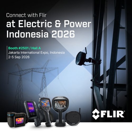
Aug 24: Teledyne FLIR will bring the new FLIR Si2a-PD to Electric & Power Indonesia 2026 — a fixed-mount acoustic imaging camera built to watch energized electrical assets around the clock. It joins the portable Si2-Series, iXX-Series, Exx-Series and T-Series cameras at Booth #2501 in Hall A, September 2–5 at the Jakarta International Expo.
Partial discharge is intermittent. A quarterly inspection catches it only if the discharge happens to be active when the inspector walks past. Closing that gap is what the Si2a-PD is for.
Si2a-PD: An Always-On Electrical Guardian
The Si2a-PD detects, locates, classifies and assesses partial discharge, corona and arcing from 0.3 m (1.0 ft) up to 200 m (656 ft). An array of 124 low-noise MEMS microphones covers a 2 kHz to 130 kHz bandwidth and overlays the acoustic image on a 12 MP color camera view with a 75° field of view.
AI-based severity assessment ranks what the camera finds and recommends an action, so the output is a maintenance decision rather than a waveform for someone to interpret. The unit is IP66-rated with VESA mounting for switchgear rooms, GIS and outdoor substations, and it feeds FLIR Assetlink™ for event tracking and integration into existing digital maintenance workflows.
“Partial discharge is often intermittent and can therefore be difficult to capture during routine inspections,” said Darrell Taylor, Business Director for Acoustics at Teledyne FLIR. “With the Si2a-PD, customers gain continuous visibility into their assets, enabling earlier detection, improved reliability, and more informed maintenance decisions.”
Si2-Series: The Portable Counterpart
Where the Si2a-PD stays mounted, the Si2-Series goes to the asset. The Si2-PD locates partial discharge in high-voltage equipment. The Si2-LD finds pressurized leaks and mechanical faults. The Si2-Pro does both and quantifies gas leaks, including hydrogen, CO₂, methane, helium, argon and ammonia. All three use the same 124-microphone array and the same 200 m reach in a one-handed camera that takes minimal training, and the Si2x models carry that capability into ATEX and HazLoc classified areas.
iXX-Series, Exx-Series and T-Series: Thermal on the Same Stand
Thermal imaging remains the fastest way to find a loose connection or an overloaded conductor before it fails. The iXX-Series — the i34 at 240 × 320 and the i64 at 480 × 640 — runs guided workflows on the camera itself and uploads results automatically to FLIR Assetlink™ for route planning or FLIR Ignite™ for trend tracking and work order generation through a connected CMMS.
The Exx-Series runs from the E54 up to the E96, which images at 640 × 480 and measures to 1500°C (2732°F), with laser-assisted autofocus on the E76, E86 and E96. The T-Series adds a 180° rotating lens platform for overhead and floor-level targets and an optional 6° telephoto lens for reading terminations from outside the fence line.
Visit Us at Electric & Power Indonesia 2026
Teledyne FLIR is at Booth #2501, Hall A, Jakarta International Expo, September 2–5, 2026. To book time with the team or to learn more about the products on display, visit www.flir.com.
24, Aug 2026
Bosgame Enters India with Kaynes Technology; Companies Sign Strategic MoU to Strengthen Computing Presence in India
Collaboration brings together BOSGAME’s intelligent computing portfolio with Kaynes Technology’s engineering, manufacturing and market execution capabilities.

The collaboration brings together BOSGAME’s product innovation and intelligent computing portfolio with Kaynes Technology’s extensive capabilities in electronics design, engineering, integrated manufacturing, testing, supply-chain management and lifecycle support.
BOSGAME’s product design has earned international recognition, including the American Good Design Award, the French Design Award and the MUSE Design Awards, underscoring the brand’s design-led engineering approach as it expands into India.

BOSGAME Design Recognition – American Good Design, French Design Award, MUSE Design Awards
Through this partnership, the companies intend to create a strong platform for introducing BOSGAME products to the Indian market, developing market channels and building a locally supported customer ecosystem.
The collaboration will also explore opportunities for product localisation, value addition and deeper participation in India’s rapidly evolving electronics ecosystem, aligned with market requirements and long-term growth opportunities.
The MoU was signed on behalf of Kaynes Technology India Limited by Mr. Jaydeep Jadav, Head – Brand Business, with Ms. Lucky Wang, Vice President, Six United, representing BOSGAME.
MoU Signing Ceremony – Kaynes Technology, BOSGAME and Six United
Mr. Jaydeep Jadav, Head – Brand Business, Kaynes Technology India Limited, said:“India is entering an exciting phase in electronics where global product innovation is increasingly being complemented by strong local engineering, manufacturing and customer support capabilities.
Our collaboration with BOSGAME is aligned with this transition. We look forward to combining BOSGAME’s product strengths with Kaynes Technology’s capabilities to build a scalable and sustainable presence for the brand in India.”
Ms. Lucky Wang, Vice President, Six United, BOSGAME, said:
“India is an important technology market with significant long-term potential. We are pleased to collaborate with Kaynes Technology, whose engineering, manufacturing and execution capabilities provide a strong foundation for our India journey. Together, we look forward to bringing innovative computing solutions closer to Indian customers and building a meaningful presence in the market.”
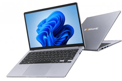
The partnership comes at a time when India is strengthening its position across the electronics value chain, with increasing emphasis on design-led manufacturing, local value creation, supply-chain resilience and technology-driven product development.
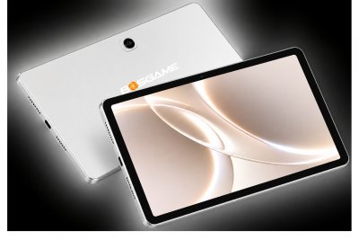
BOSGAME Tablets and Mini PC
By combining international product innovation with Indian engineering and manufacturing capabilities, Kaynes Technology and BOSGAME aim to create a strong foundation for the next phase of BOSGAME’s growth in India.

BOSGAME Product Lineup – Laptop, Tablet and Mini PC